
Each simulated cell channel must be electrically isolated so multiple channels can be connected in series for cell-string BMS inputs. Isolation is typically achieved using transformer-based DC-DC converters and digital isolators for the control signals.
BMS hardware-level design
Battery Emulator Circuit
A battery emulator circuit architecture uses isolated programmable channels, precision voltage sources, source-sink behavior, controlled fault paths, and calibration circuits to accurately reproduce battery cell electrical characteristics for BMS test benches. This guide covers the circuit topology, isolation design, component selection, and layout considerations for building or selecting a battery emulator for BMS tester applications.
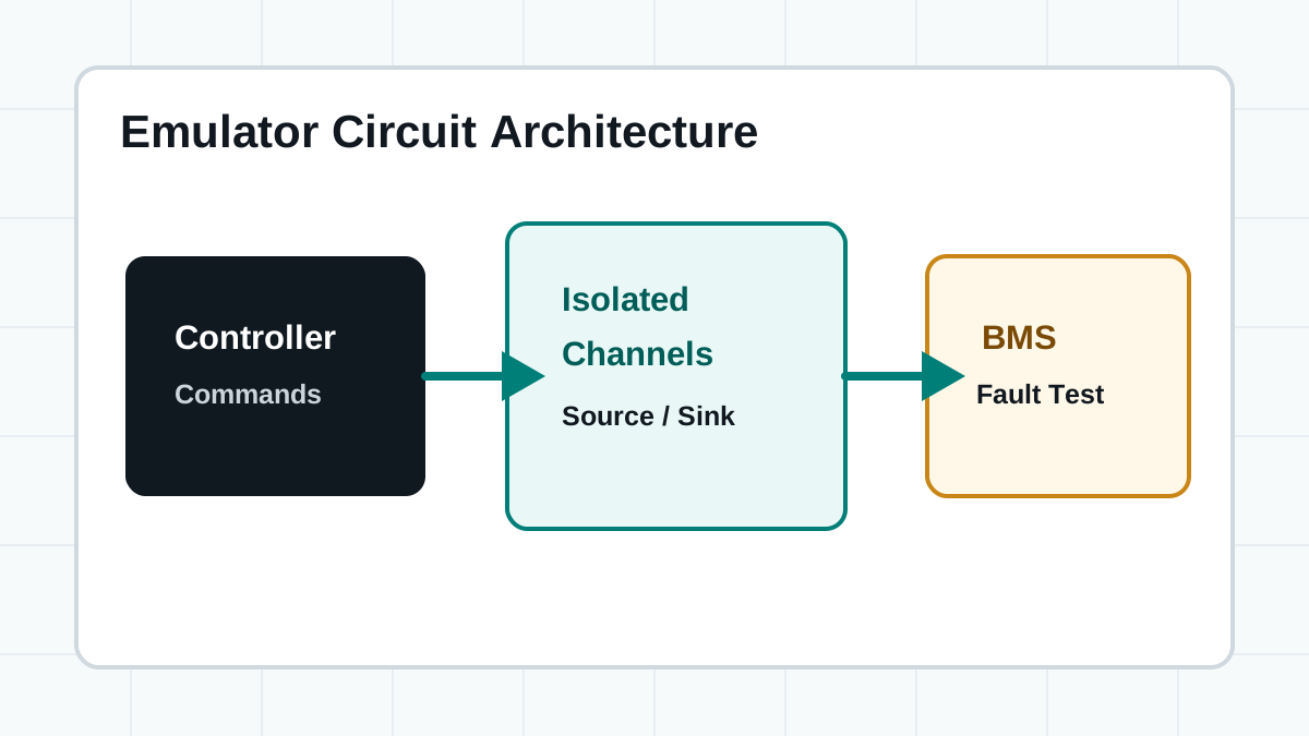
- Isolated programmable channels for series cell simulation
- Precision op-amp based voltage source with 4-wire sensing
- Source and sink behavior for balancing-related tests
- Controlled open, short, reverse, and imbalance fault paths
- Over-voltage clamp and reverse polarity protection
Short answer: A battery emulator circuit architecture must mimic series-stacked battery cells without making the test bench unsafe or inaccurate. In practice, that means isolated channels, stable precision voltage control, current source-sink capability where required, software-controlled fault states, and calibration circuits to maintain accuracy over temperature and time. The core circuit typically consists of a programmable voltage source (usually op-amp based), a current measurement stage, an isolation barrier (magnetic or capacitive), fault injection relays or switches, and a communication interface to the host battery simulator software. For multi-cell BMS testing, multiple channels are stacked in series, requiring channel-to-channel isolation ratings of 100V to 1000V depending on the target battery pack voltage. Additional circuitry handles safety functions such as over-voltage clamping, reverse polarity protection, and current limiting to protect both the emulator and the BMS under test.
Working principles
Core Parts of a Battery Emulation Architecture
Industrial battery emulation requires more than a standard DC power supply. A BMS bench usually needs isolation, repeatability, controllable current behavior, and reliable fault paths. The following core subsystems are present in nearly all professional battery emulator designs.
BMS tests require the simulator to source current (simulate discharge), sink current (simulate charge or active balancing), or support bidirectional behavior depending on the selected product series and BMS architecture.
Fault paths reproduce open circuit, short circuit, reverse connection, and imbalance cases so protection logic can be checked repeatedly. Solid-state switches or electromechanical relays control these fault conditions under software command.
The emulator must maintain voltage accuracy better than the BMS voltage reading accuracy, typically ±1 mV to ±5 mV, across the full operating temperature range and over long test durations.
When the BMS enables passive balancing (drawing current from the cell), the emulator voltage must settle to the new steady state within milliseconds to avoid false over-voltage or under-voltage triggers during testing.
Offset and gain drift in op-amps, references, and ADCs require periodic calibration. Production emulator circuits include calibration DACs or trim registers accessible through the communication interface.
Equivalent circuit model
Thevenin Equivalent Circuit Model in Emulation
The Thevenin equivalent circuit is the most widely used electrical model for lithium-ion battery cells in BMS algorithms. Understanding this model is essential for designing emulator circuits that can reproduce realistic cell behavior beyond simple DC voltage sources.
The Thevenin model represents a battery cell as an open-circuit voltage source Voc in series with an ohmic resistance Rs (representing electrolyte and electrode resistance), followed by a parallel RC branch (Rp, Cp) that models the polarization and diffusion effects. The terminal voltage Vt = Voc − I·Rs − Vp, where Vp is the voltage across the parallel RC branch.
A basic emulator implements only the Voc source (programmable voltage). More advanced emulators add switchable series resistance (Rs) using a MOSFET or precision resistor network to simulate the ohmic drop during load transients. Some research-grade emulators also include a programmable RC branch to simulate polarization effects, though this adds significant circuit complexity.
| Thevenin Parameter | Typical Li-ion Range | Circuit Component | Emulation Approach |
|---|---|---|---|
| Voc (Open circuit voltage) | 3.0V – 4.2V | Precision voltage source | Op-amp + DAC + feedback |
| Rs (Ohmic resistance) | 1mΩ – 50mΩ | Series MOSFET or resistor | Programmable current-dependent drop |
| Rp (Polarization resistance) | 0.1mΩ – 10mΩ | Parallel resistor network | Optional; complex for real-time |
| Cp (Polarization capacitance) | 1kF – 10kF (equivalent) | Simulated with DSP | Usually modeled in software |
Design note: For most BMS hardware-in-the-loop testing, implementing the full Thevenin RC branch in hardware is unnecessary because BMS algorithms model the cell dynamics in software. The emulator needs to accurately reproduce the DC voltage and the fast transient response (Rs effect) when the BMS enables balancing. Adding a programmable series resistance of 0–100mΩ per channel is usually sufficient for battery cell emulator applications.
Voltage source design
Operational Amplifier Based Voltage Source Design
The precision voltage source is the core of a battery emulator channel. Most professional designs use an op-amp based topology because it provides low output impedance, programmable voltage via DAC control, and the ability to source and sink current when configured as a two-quadrant output.
The simplest implementation uses a precision op-amp in a unity-gain buffer configuration, with the noninverting input driven by a DAC and the output buffered by a power MOSFET stage. The op-amp forces the output voltage to match the DAC setpoint by comparing the feedback voltage (from a Kelvin sense point) with the DAC voltage. A typical design uses a 16-bit or 18-bit DAC to achieve 1 mV resolution over a 0–5V range.
A standard op-amp voltage source can only source current (push current into the load). To also sink current (absorb current from an external source such as an active balancing circuit), the output stage must be designed as a two-quadrant source: typically a push-pull MOSFET pair (N-channel and P-channel) driven by the op-amp. This allows the emulator to both deliver current to the BMS and absorb current from the BMS without the output voltage deviating from the setpoint.
Key Op-Amp Selection Criteria
- Input offset voltage: < 50 µV to minimize DC error without excessive calibration overhead.
- Gain-bandwidth product: > 1 MHz to ensure stable feedback loop response with capacitive loads introduced by cables and BMS input filters.
- Output current capability: > 100 mA per channel to support passive balancing currents up to 200 mA (typical for automotive BMS).
- Rail-to-rail input and output: Necessary to utilize the full DAC range without additional level-shifting circuits.
- Low 1/f noise: < 10 nV/√Hz at 1 kHz to maintain voltage stability during sensitive BMS voltage reading tests.
A common op-amp choice for battery emulator designs is the OPA2188 (precision, low offset, rail-to-rail) or the ADA4528 (zero-drift, ultralow noise). The output stage typically uses a MOSFET pair such as the IRFZ44N (N-channel) and IRF4905 (P-channel) for higher current capability, with gate drive resistors to prevent oscillation. The difference between emulator and simulator often comes down to how sophisticated this voltage source design is.
Galvanic isolation
Isolation Design: Why and How Each Channel is Isolated
When multiple emulator channels are connected in series to simulate a battery string, each channel's output must be galvanically isolated from the others and from the control system. Without isolation, connecting the outputs in series would short-circuit the internal power supplies and damage the emulator.
Why Isolation is Required
In a battery pack, each cell "floats" at a different potential relative to the pack negative terminal. Cell 1 is at 3.6V, cell 2 is at 7.2V, cell 3 is at 10.8V, and so on. To simulate this, each emulator channel must also float at its respective stack potential. The control signals (SPI, I2C, UART) and power supplies for each channel must cross an isolation barrier. The isolation rating must exceed the maximum stack voltage — for a 1000V EV battery pack with 200 cells, each channel needs > 1000V isolation from the ground-referenced controller.
Isolation Implementation Methods
Each channel is powered by its own isolated DC-DC converter (e.g., Traco Power TEL 3 series or Recom RxxPxx series). These provide 1000V to 3000V isolation between input and output. The converter's output is referenced to the channel's floating ground, which is connected to the previous channel's positive terminal in the series stack.
Control signals cross the isolation barrier through digital isolators such as the ISO7741 (4-channel digital isolator, 3000V isolation) or ADuM1401. For SPI control, three isolators are needed (CS, SCLK, MOSI one direction; MISO the other direction). Capacitive isolation (Silicon Labs Si86xx) and magnetic isolation (Analog Devices iCoupler) are both commonly used.
Older designs use optocouplers (e.g., 6N137, HCPL-2630) for signal isolation. While optocouplers provide good isolation (up to 5000V), they have slower speed, higher power consumption, and suffer from CTR (current transfer ratio) degradation over temperature and lifetime. Modern designs prefer digital isolators for better performance and reliability.
Safety consideration: Isolation creepage and clearance distances on the PCB must meet IEC 60950 or IEC 62368 standards. For 1000V working voltage, creepage > 6.4mm is typically required. This affects PCB layout significantly — the battery pack simulator PCB must have isolation slots (mills) between channels to increase creepage distance. Always consult the relevant safety standard for your target market.
Measurement accuracy
4-Wire Kelvin Connection Design and PCB Layout
Achieving ±1 mV accuracy in cell voltage emulation requires eliminating voltage drops in cables, connectors, and PCB traces. The 4-wire Kelvin connection method separates the high-current force lines from the voltage-sense lines, allowing the emulator to regulate the voltage precisely at the BMS connector rather than at the emulator output.
Kelvin Connection Principle
In a 2-wire connection, the voltage regulator senses the output voltage at the emulator PCB, but the voltage at the BMS input may be different due to IR drop in the force wires (Vdrop = I · Rwire). For example, with 200 mA balancing current and 0.5Ω total wire resistance, the voltage error is 100 mV — completely unacceptable for BMS testing. In a 4-wire Kelvin connection, two separate wires (or PCB traces) are used for force (F+, F-) and two for sense (S+, S-). The op-amp feedback loop uses only the sense lines, so the regulator automatically compensates for the voltage drop in the force lines.
PCB Layout Considerations for Kelvin Connections
- Force and sense trace separation: On the PCB, force and sense traces must be routed separately from the op-amp output to the output connector. They should only be connected at the connector (or at a Kelvin pad very close to the connector).
- Sense trace impedance: Sense lines carry negligible current (< 1 mA), so they can be thin traces. However, they are sensitive to noise pickup. Route sense traces as a differential pair, away from switching nodes (DC-DC converters, digital signals).
- Connector selection: Use connectors that support 4-wire connections, such as standard 4-pin headers or specialized Kelvin connectors. Each emulator channel needs 4 wires to the BMS: Force+, Sense+, Force-, Sense- (though Force- and Sense- are often shared as a common ground).
- Thermal management: Force traces carry the balancing current and must be sized for current capacity. A 200 mA current requires at least 0.5 mm trace width on 1 oz copper (more for higher currents). Consider using external PCB copper or copper busbars for high-current channels.
- Ground loops: When stacking channels in series, the sense ground (S-) of one channel connects to the sense ground of the next channel at the BMS side, not at the emulator side. This prevents ground loops that can introduce measurement errors.
For battery simulator test equipment, the cable between the emulator and the BMS is often the largest source of error. Using twisted-pair cables for the sense lines (twisted with the corresponding force line) reduces noise pickup. Shielded cables may be necessary in electromagnetically noisy environments such as EV powertrain test cells.
Two-quadrant operation
Source-Sink (Two-Quadrant) Circuit Topology
A battery emulator channel must be able to both source current (act as a power source, like a discharging battery) and sink current (act as a load, like a charging battery or an active balancing sink). This two-quadrant operation is fundamental to testing both passive and active balancing circuits in modern BMS designs.
Quadrant Operation Diagram Description
In the voltage-current (V-I) plane, a two-quadrant source operates in Quadrant I (positive voltage, positive current = sourcing) and Quadrant IV (positive voltage, negative current = sinking). The op-amp controls the output voltage, and the current direction is determined by the external circuit (the BMS balancing load or active balancing source). The emulator must maintain accurate voltage regulation in both directions.
Push-Pull Output Stage Design
When the BMS draws current from the emulator (passive balancing), the op-amp drives the N-channel MOSFET (source mode) to deliver current from the channel's local power supply to the output. The op-amp increases the gate voltage until the output voltage (measured by the sense lines) matches the DAC setpoint. Current limiting is typically implemented by sensing the MOSFET current and reducing the gate drive if the current exceeds the programmed limit.
When an external source (such as an active balancing circuit) pushes current into the emulator, the op-amp drives the P-channel MOSFET to sink that current to the channel's local ground. The op-amp must operate in closed-loop regulation even when current is flowing backward. This requires the op-amp to have a bipolar output stage or a separate sink driver circuit. Some designs use a separate op-amp for sink mode to improve stability.
Stability Considerations in Two-Quadrant Operation
The feedback loop stability of a two-quadrant source is more complex than a single-quadrant source because the loop dynamics change depending on the current direction and magnitude. The output capacitance (including cables and BMS input capacitance) forms a pole with the output resistance. When the load is capacitive (as most BMS inputs are, due to input RC filters), the phase margin can degrade, causing overshoot or oscillation. Compensation networks (RC snubbers, feedback capacitors) are essential. A staggered compensation approach — different compensation for source vs. sink mode — can be implemented using analog switches to select the appropriate compensation network based on the measured current direction.
For high-performance battery cell simulator applications, a linear op-amp approach is preferred over a switching (buck/boost) approach because the linear design has much lower output noise and faster transient response. However, the linear approach has lower efficiency. For high-current channels (> 1A), a hybrid approach using a switched-mode pre-regulator followed by a linear post-regulator can improve efficiency while maintaining low noise.
Parameters
Key Specifications for Circuit Performance
When evaluating or designing a battery emulator circuit, the following specifications determine whether the emulator can accurately test the target BMS. Understanding these parameters helps in selecting the right battery simulator for a specific application.
| Parameter | Typical Target | Why it matters | BMS testing impact |
|---|---|---|---|
| Channel isolation voltage | 100V – 1000V | Determines whether channels can be used safely in series for high-voltage pack simulation. | Critical for multi-cell BMS inputs and pack-equivalent strings. Insufficient isolation causes safety hazards and measurement errors. |
| Voltage accuracy | ±1 mV to ±5 mV | Determines how precisely each simulated cell can be set and read back. | Important for over-voltage/under-voltage threshold testing, calibration validation, and SoC estimation testing. |
| Voltage resolution | 0.1 mV to 1 mV | Smallest voltage step the emulator can produce. | Fine resolution enables gradual voltage ramps to test BMS voltage hysteresis and filtering behavior. |
| Transient settling time | < 1 ms to < 10 ms | Time for output to settle within 1 mV after a load step (e.g., balancing on/off). | Slow settling can cause false BMS fault triggers during balancing tests. |
| Source-sink current | 0 – 300 mA (source), 0 – 300 mA (sink) | Maximum current the channel can source or sink while maintaining voltage regulation. | Must exceed the maximum BMS balancing current. Typical passive balancing is 50–200 mA per cell. |
| Fault simulation types | Open, short, reverse, imbalance | Determines which abnormal wiring or cell states can be reproduced. | Essential for functional safety validation (ISO 26262) and protection logic verification. |
| Temperature drift | < 50 µV/°C | Voltage change per degree of ambient temperature change. | Important for test benches that operate over wide temperature ranges or without temperature-controlled environments. |
Protection circuits
Safety Circuits: Over-Voltage Clamp, Reverse Polarity Protection, Current Limiting
Battery emulator circuits operate in close proximity to expensive BMS hardware and, in some test configurations, real battery packs. Comprehensive protection circuits are essential to prevent damage to the emulator, the BMS, and the test equipment.
If the op-amp fails or the DAC sends an incorrect setpoint, the output voltage could exceed the BMS absolute maximum rating (typically 5V – 6V for a 3.6V nominal cell). An over-voltage clamp circuit uses a precision voltage reference (e.g., 4.5V) and a comparator to detect over-voltage, then activates a crowbar SCR or MOSFET to clamp the output to a safe voltage. A passive clamp using a Zener diode (5.6V) provides backup protection even if the active clamp fails. The clamp must be fast (< 1 µs response) to protect the BMS before damage occurs.
If the test engineer accidentally reverses the emulator output cables, the BMS could be subjected to negative voltage, or the emulator could be damaged. A series Schottky diode (e.g., SB5100) provides simple reverse polarity protection with ~0.4V forward drop. For lower loss, an N-channel MOSFET in the return path (with gate controlled by the polarity of the input) provides near-zero forward voltage drop while still blocking reverse polarity. Some designs use an ideal diode controller (e.g., LTC4372) for this purpose.
Each channel should have both a fixed hardware current limit (for safety) and a programmable software current limit (for test flexibility). The hardware limit uses a sense resistor and comparator to rapidly disconnect the output if current exceeds, say, 500 mA. The software limit is implemented in the DAC/op-amp control loop and can be set per test scenario. Bidirectional current limiting (for both source and sink modes) requires two separate sense circuits or a bidirectional current sense amplifier (e.g., INA240).
Additional Protection Features
- Thermal protection: Each power MOSFET should have a temperature sensor (or use the built-in thermal protection of the MOSFET driver). If the temperature exceeds 85°C (or a configurable threshold), the channel should reduce output current or shut down.
- Output short-circuit protection: If the BMS input is shorted (which can happen during fault testing or wiring errors), the emulator must survive without damage. A foldback current limit (where the current limit reduces as the output voltage drops) prevents excessive power dissipation during a short circuit.
- Isolation fault detection: Some emulator designs include circuitry to detect if the isolation barrier has failed (which could expose the control system to high voltage). This can be implemented by periodically measuring the leakage current across the isolation barrier using a high-value resistor divider and a comparator.
Accuracy maintenance
Calibration and Drift Compensation Circuit Design
Even the best analog circuit drifts over time and temperature. Op-amp input offset voltage drifts by 1–10 µV/°C, voltage references drift by 10–50 ppm/°C, and resistor values change with temperature and aging. A production battery emulator must include calibration circuits to correct these errors and maintain specified accuracy throughout the product lifecycle.
Calibration Architecture
A typical calibration approach uses a precision reference voltage (applied to the input during calibration) and measures the actual output using a high-accuracy external multimeter. The calibration software records the offset and gain errors at multiple setpoints (e.g., 2.5V, 3.0V, 3.6V, 4.2V, 5.0V) and stores correction coefficients in non-volatile memory (EEPROM or flash). During normal operation, the battery simulator software applies these coefficients to the setpoint before sending it to the DAC.
Hardware Calibration Circuits
Some precision op-amps include a dedicated offset trim pin. For those that don't, a small correction voltage can be injected into the op-amp summing node using a 12-bit or 16-bit trim DAC (e.g., AD5160 digital potentiometer or LTC2630 DAC). The trim range is typically ±10 mV, which is sufficient to correct offset errors from the op-amp, DAC, and voltage reference.
Higher-end emulator channels include an on-board precision voltage reference (e.g., LTZ1000 or ADR4525, 0.02% initial accuracy, 2 ppm/°C drift) that can be multiplexed to the output for self-calibration. The emulator can periodically measure its own output against this reference and update the calibration coefficients without external equipment. This is valuable for automated test benches that run unattended for long periods.
Temperature Compensation
If the emulator operates in a temperature-controlled environment (e.g., a climate chamber for BMS temperature testing), the calibration coefficients can be indexed by temperature. A temperature sensor (e.g., LM75 or TMP117) on each channel PCB measures the local temperature, and the software interpolates between calibration coefficients stored for different temperatures. This approach can reduce temperature-induced voltage error to < 0.1 mV across a 0–70°C range.
Component selection
Component Selection Guide for Battery Emulator Circuits
The performance of a battery emulator circuit is only as good as its components. This section provides guidance on selecting critical components for a professional-grade design. All components should be automotive-grade (AEC-Q100 or AEC-Q200 qualified) for EV BMS test applications.
Operational Amplifiers
| Parameter | Recommended Value | Example Parts | Notes |
|---|---|---|---|
| Input offset voltage | < 50 µV | OPA2188, ADA4528-2, LTC2050 | Zero-drift types eliminate 1/f noise and minimize offset drift. |
| Input bias current | < 10 nA | ADA4528-2 (50 pA), LTC2050 (10 pA) | Low bias current reduces errors from source resistance. |
| Gain bandwidth product | > 1 MHz | Most precision op-amps meet this | Higher GBW improves transient response with capacitive loads. |
| Supply voltage range | 5V – 36V (single supply) | OPA2188 (4V–36V), ADA4528 (2.7V–5.5V) | Must accommodate the local isolated supply voltage. |
Power MOSFETs (Output Stage)
| Parameter | Recommended Value | Example Parts | Notes |
|---|---|---|---|
| Drain-source voltage (Vds) | > 30V | IRFZ44N (60V), IRF4905 (-55V), BSC016N04LS (40V) | Must exceed the maximum channel output voltage plus margin. |
| Continuous current (Id) | > 5A | IRFZ44N (49A), IRF4905 (-74A) | Provides margin over the 0.3A typical balancing current requirement. |
| On-resistance (Rds(on)) | < 20 mΩ | BSC016N04LS (1.6 mΩ), IRFZ44N (17.5 mΩ) | Lower Rds(on) reduces power dissipation and thermal drift. |
| Gate charge (Qg) | < 50 nC | BSC016N04LS (19 nC), IRFZ44N (67 nC) | Lower Qg improves switching speed and reduces op-amp drive requirement. |
ADC and DAC Considerations
- DAC resolution: 16-bit minimum (0.15 mV resolution over 0–5V range). 18-bit or 20-bit preferred for highest accuracy emulators. Multi-channel DACs (e.g., AD5668, 8-channel 16-bit) reduce component count.
- DAC voltage reference: The DAC reference directly determines the output voltage accuracy. Use a precision reference such as the REF5050 (5.0V, 3 ppm/°C, 0.05% initial accuracy) or ADR4525 (2.5V, 2 ppm/°C). The reference should be located as close to the DAC as possible, with a clean analog power supply.
- ADC for readback: Each channel should include an ADC to read back the actual output voltage (for closed-loop correction and diagnostics). A 16-bit or 18-bit ADC (e.g., ADS1115, ADS1015, or higher-performance LTC2450) with an I2C or SPI interface provides readback accuracy better than the DAC setpoint accuracy.
- Isolation for ADC/DAC: If the DAC and ADC are on the isolated side (floating with the channel), they must be controlled through the digital isolator. If they are on the ground-referenced side, the analog signals must cross the isolation barrier using isolated amplifiers (e.g., AMC1301, AMC1200) — a more complex but sometimes preferable approach because it keeps the precision components on the ground-referenced side where temperature is more controlled.
For designers building custom battery simulator fundamentals into their test systems, careful attention to component derating is essential. MOSFETs should be derated to 50% of their maximum Vds and Id ratings. Op-amps should operate within their specified input common-mode range at all times (which can be challenging in a single-supply design where the input is near ground). Resistors should be 0.1% tolerance, 25 ppm/°C or better, with a low-noise characteristic (metal film, not thick film which can have excess noise and voltage coefficient errors).
FaithTech hardware
Industrial Modular Test Circuits
FaithTech produces a range of battery emulator hardware that implements the circuit principles described in this guide. These systems are designed for production test environments, R&D labs, and automated validation benches.
Multi-channel isolated battery cell simulation for BMS validation and production-oriented test work. Each channel provides ±5 mV accuracy, 300 mA source/sink capability, and 1000V channel-to-channel isolation. Software-controlled fault injection enables comprehensive protection testing.
Bidirectional battery simulator paths for projects that need source-sink behavior and active balancing validation. These models add programmable series resistance (to simulate cell internal resistance) and faster transient response (< 500 µs settling) for advanced BMS algorithm testing.
Combines battery simulation hardware with signal checks, communication (CAN, LIN, UART), automation scripts, and reporting workflows. The BMS tester software integrates with NI LabVIEW, Python, and MATLAB for custom test development.
FAQ
Battery Emulator Circuit FAQ
Why can't I use a regular power supply circuit for BMS testing?
A standard power supply may be useful for simple power checks, but BMS testing often needs many isolated cell channels, controlled imbalance, fault states, and repeatable automation. A standard supply also lacks the fast transient response needed when the BMS switches balancing on and off. Additionally, standard supplies are not designed to be stacked in series at high voltages, creating isolation and safety issues.
What is the difference between active and passive balancing in BMS tests?
Passive balancing usually dissipates excess energy through a resistor controlled by the BMS, requiring the emulator to sink the balancing current while maintaining accurate voltage. Active balancing moves energy between cells using charge pumps or inductors, requiring the emulator to both source and sink current and to respond to bidirectional energy transfer. The battery cell emulator must support the appropriate current direction for the BMS balancing type.
How is transient response measured in these circuits?
It is measured by applying a step change in load current (e.g., from 0A to 1A, simulating balancing turn-on) and timing how long it takes the cell circuit voltage to stabilize within a specified millivolt band (e.g., ±2 mV of the target). An oscilloscope with high-precision differential probes is typically used. The settling time should be < 5 ms for most BMS applications to prevent false fault triggers.
Which FaithTech circuits should I evaluate?
Review the FT8330 or FT8331 for standard passive BMS testing, and the FT8340 or FT8350 series for bidirectional active balancing requirements. For high-channel-count pack simulation, the FT8330 series supports stacking up to 256 channels in a single system with synchronized updating.
What is the Thevenin equivalent model and why does it matter for emulator design?
The Thevenin model represents a battery as an open-circuit voltage source in series with a resistance (Rs) and a parallel RC branch (Rp, Cp) for polarization. While most BMS testing only requires accurate DC voltage emulation, some advanced test scenarios (such as testing BMS SOC estimation algorithms that account for polarization voltage) benefit from an emulator that can simulate the RC time constant. This requires adding a programmable current-dependent voltage drop and, optionally, a simulated RC response using a DSP-controlled output.
How do 4-wire Kelvin connections improve accuracy in battery emulation?
In a 2-wire connection, the voltage regulator senses the output at the emulator PCB, but the voltage at the BMS input differs due to IR drop in the wires (V = I · R). With 200 mA balancing current and 1Ω total wire resistance, this error is 200 mV — larger than the BMS voltage threshold hysteresis. A 4-wire Kelvin connection feeds back the actual voltage at the BMS connector to the op-amp, automatically compensating for wire resistance. This enables ±1 mV accuracy even with long cables and high balancing currents. Proper battery simulator test equipment always uses Kelvin connections for the cell voltage outputs.
What isolation voltage rating do I need for my emulator channels?
The isolation voltage must exceed the maximum stack voltage of the BMS under test. For a 400V EV battery pack (about 96 cells), each channel needs at least 500V isolation (with safety margin to 1000V). For a 12V lead-acid battery (6 cells), 60V isolation is sufficient. Always derate the isolation rating by 50% for safety (a 1000V rated isolator is used for up to 500V working voltage). Check the relevant safety standard (IEC 60950, IEC 62368, or UL 61010) for the specific creepage and clearance requirements for your working voltage.
Related guides
Related Emulation Topics
Continue exploring battery emulator and BMS testing topics with these related technical guides.
Talk to FaithTech
Need high-precision emulator circuits for your test bench?
Share your cell string count, isolation voltage requirements, balancing currents, accuracy targets, and hardware control interfaces. FaithTech engineers can help match the right card architecture to your BMS validation requirements. Whether you need basic passive balancing support or advanced active balancing emulation with programmable internal resistance, FaithTech has a solution.